Layer stack
Copper, mask, silkscreen, paste, drill, route, document and board-outline roles from the job matrix, with the board thickness and inner copper depths the job states.
 AGBoard - PCBEditor
Complete ODB++ PCB jobs
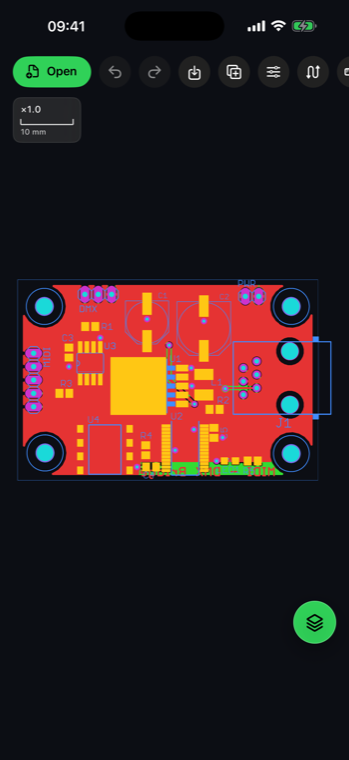
Open an ODB++ folder or archive as one structured PCB project. Inspect the stackup, expanded panels, component packages, pins and logical nets without uploading the design.
folder.zip.tgz.tar.tar.gz.7z.tar.xzAGBoard reads the ODB++ matrix, steps, layers, features, component data and EDA net information. Panel steps are expanded into the board view while their source data remains organized by layer.
Large and compressed jobs open quickly, with progress feedback, and use the same accelerated canvas as Gerber projects, making dense production data practical to inspect on an iPhone or iPad.
Copper, mask, silkscreen, paste, drill, route, document and board-outline roles from the job matrix, with the board thickness and inner copper depths the job states.
Step repetitions, lines, arcs, pads, surfaces, routed profiles, cutouts and drill features.
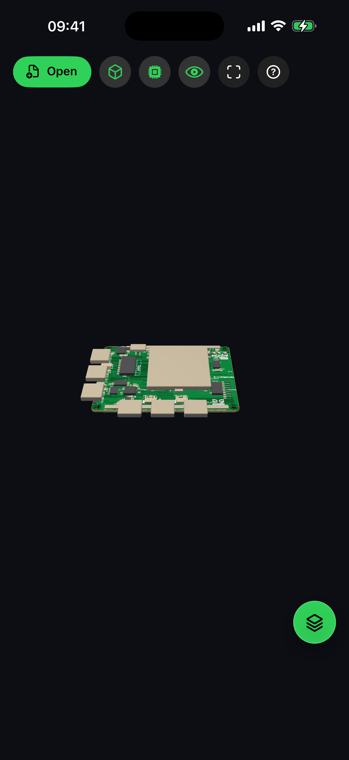
Component references, packages, pins, top or bottom placement and logical net relationships. In 3D, parts take the height and package outline the job gives them, and the board takes the step profile as its outline — not a panel frame.
The same touch-first tools stay available from a phone or a larger iPad workspace.
AGBoard accepts an ODB++ directory and common .zip (ZIP64 included), .7z, .tgz, .tar, .tar.gz, .tar.xz and .tar.bz2 archives.
Yes. Panel steps are expanded, while supported component, package, pin and EDA net data power search and highlighting.
No. Extraction, parsing and rendering happen locally on the device.
Download AGBoard on iPhone or iPad. Five file opens are included before an AGBoard Pro subscription is required.